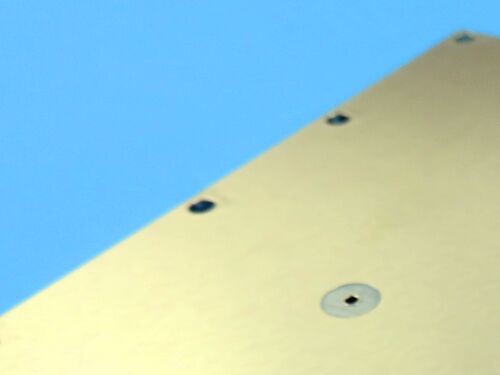
logo
prodotti
Dettagli dei prodotti
Casa. > prodotti >
F4BTMS615 PCB Double-layer 0.3mm 20um Via Plating Immersion Tin

F4BTMS615 PCB Double-layer 0.3mm 20um Via Plating Immersion Tin

MOQ: 1 pz
prezzo: USD9.99-99.99
Imballaggio standard: Sacchetti sottovuoto+Cartoni
Periodo di consegna: 8-9 giorni lavorativi
Metodo di pagamento: T/T
Capacità di approvvigionamento: 5000 pezzi al mese
Informazioni dettagliate
Luogo di origine
Cina
Marca
Bicheng
Certificazione
UL, ISO9001, IATF16949
Numero di modello
BIC-470.V1.0
Materiale di base:
F4BTMS615
Conteggio degli strati:
2 strati
Spessore del PCB:
0,3 mm
Dimensioni del circuito stampato:
45,8 mm x 102,1 mm, 1 pezzo, con una tolleranza di +/- 0,15 mm
Maschera per saldatura:
NO
Serigrafia:
NO
Peso del rame:
1 oncia (1,4 mil) per gli strati esterni
Finitura superficiale:
Stagno per immersione
Evidenziare:

double-layer RF PCB board

,

0.3mm immersion tin PCB

,

20um via plating PCB

Descrizione del prodotto

This 2-layer rigid PCB adheres to international industry standards to ensure dependable performance. It adopts F4BTMS615 as its base substrate, which is specifically designed to fulfill the strict requirements of aerospace, microwave, and RF applications, boasting superior electrical, mechanical, and thermal properties.


PCB Specification

Item Details
Base Material F4BTMS615
Layer Count 2 layers
Board Dimensions 45.8mm x 102.1mm, 1 Piece, with a tolerance of +/- 0.15mm
Minimum Trace/Space 4/5 mils
Minimum Hole Size 0.3mm
Finished Board Thickness 0.3mm
Finished Copper Weight 1 oz (1.4 mils) for outer layers
Via Plating Thickness 20 μm
Surface Finish Immersion Tin
Silkscreen No silkscreen is applied to either the top or bottom layer
Solder Mask No solder mask is applied to either the top or bottom layer
Quality Control A 100% electrical test is performed before shipment


PCB Stack-up

The 2-layer rigid PCB is designed with an optimized stackup structure, which is customized to enhance mechanical stability, electrical performance, and thermal conductivity. The layers from top to bottom are as follows:

Layer Specifications
Copper Layer 1 35 μm
F4BTMS615 Core 0.254 mm (10 mil)
Copper Layer 2 35 μm


Artwork and Quality Standard

Artwork Format Supplied: Gerber RS-274-X, the global industry standard for PCB manufacturing, ensuring compatibility with mainstream equipment and software for accurate design data transmission and reduced deviations.


Quality Standard: IPC-Class-2, a widely accepted benchmark with strict requirements for material, dimension, electrical and mechanical performance to meet high-performance electronic applications with moderate reliability.


F4BTMS615 PCB Double-layer 0.3mm 20um Via Plating Immersion Tin 0


Availability

This PCB is offered for global shipping, with support for international logistics to cater to the varied needs of overseas projects and guarantee prompt delivery.


Introduction to F4BTMS Base Material

The F4BTMS series is an upgraded iteration of the F4BTM series, with technological advancements in material formulation and manufacturing techniques. By adding a substantial quantity of ceramics and reinforcing with ultra-thin, ultra-fine glass fiber cloth, the material’s performance has been significantly enhanced, and it offers a wider range of dielectric constants. It is a high-reliability material suitable for aerospace use and can serve as a substitute for similar foreign products.


Through the integration of a small amount of ultra-thin, ultra-fine glass fiber cloth and a large quantity of uniformly dispersed special nano-ceramics mixed with polytetrafluoroethylene resin, the material reduces the adverse impact of glass fiber on electromagnetic wave propagation. This leads to lower dielectric loss, improved dimensional stability, reduced X/Y/Z anisotropy, an expanded usable frequency range, enhanced electrical strength, and increased thermal conductivity. Furthermore, it possesses an excellent low coefficient of thermal expansion and stable dielectric temperature characteristics. The F4BTMS series is equipped with RTF low-roughness copper foil as standard, which lowers conductor loss and ensures excellent peel strength, and it is compatible with both copper and aluminum substrates.


Key Features of F4BTMS615 Material

Key Features Specifications & Descriptions
Dielectric Constant (Dk) 6.15 at 10GHz
Dissipation Factor 0.0020 at 10GHz; 0.0023 at 20GHz
Coefficient of Thermal Expansion (CTE) X-axis: 10 ppm/°C; Y-axis: 12 ppm/°C; Z-axis: 40 ppm/°C (-55°C to 288°C)
Thermal Coefficient of Dk -96 ppm/°C (-55°C to 150°C)
Thermal Conductivity 0.67 W/mk
Moisture Absorption 0.1%


Typical Applications

-Aerospace equipment, space and cabin equipment

-Microwave and RF devices

-Radar, military radar

-Feed networks

-Phase-sensitive antennas, phased array antennas

-Satellite communications, and other related applications


Conclusion

This 2-layer rigid PCB demonstrates outstanding high-frequency performance, structural stability, and manufacturability, supported by the superior properties of F4BTMS615 material and strict pre-shipment quality control measures.


These characteristics make it an ideal and reliable option for global manufacturers involved in aerospace, microwave, radar, and satellite communication projects, especially those that demand stable dielectric properties, low loss and excellent dimensional stability.


F4BTMS615 PCB Double-layer 0.3mm 20um Via Plating Immersion Tin 1

prodotti
Dettagli dei prodotti
F4BTMS615 PCB Double-layer 0.3mm 20um Via Plating Immersion Tin
MOQ: 1 pz
prezzo: USD9.99-99.99
Imballaggio standard: Sacchetti sottovuoto+Cartoni
Periodo di consegna: 8-9 giorni lavorativi
Metodo di pagamento: T/T
Capacità di approvvigionamento: 5000 pezzi al mese
Informazioni dettagliate
Luogo di origine
Cina
Marca
Bicheng
Certificazione
UL, ISO9001, IATF16949
Numero di modello
BIC-470.V1.0
Materiale di base:
F4BTMS615
Conteggio degli strati:
2 strati
Spessore del PCB:
0,3 mm
Dimensioni del circuito stampato:
45,8 mm x 102,1 mm, 1 pezzo, con una tolleranza di +/- 0,15 mm
Maschera per saldatura:
NO
Serigrafia:
NO
Peso del rame:
1 oncia (1,4 mil) per gli strati esterni
Finitura superficiale:
Stagno per immersione
Quantità di ordine minimo:
1 pz
Prezzo:
USD9.99-99.99
Imballaggi particolari:
Sacchetti sottovuoto+Cartoni
Tempi di consegna:
8-9 giorni lavorativi
Termini di pagamento:
T/T
Capacità di alimentazione:
5000 pezzi al mese
Evidenziare

double-layer RF PCB board

,

0.3mm immersion tin PCB

,

20um via plating PCB

Descrizione del prodotto

This 2-layer rigid PCB adheres to international industry standards to ensure dependable performance. It adopts F4BTMS615 as its base substrate, which is specifically designed to fulfill the strict requirements of aerospace, microwave, and RF applications, boasting superior electrical, mechanical, and thermal properties.


PCB Specification

Item Details
Base Material F4BTMS615
Layer Count 2 layers
Board Dimensions 45.8mm x 102.1mm, 1 Piece, with a tolerance of +/- 0.15mm
Minimum Trace/Space 4/5 mils
Minimum Hole Size 0.3mm
Finished Board Thickness 0.3mm
Finished Copper Weight 1 oz (1.4 mils) for outer layers
Via Plating Thickness 20 μm
Surface Finish Immersion Tin
Silkscreen No silkscreen is applied to either the top or bottom layer
Solder Mask No solder mask is applied to either the top or bottom layer
Quality Control A 100% electrical test is performed before shipment


PCB Stack-up

The 2-layer rigid PCB is designed with an optimized stackup structure, which is customized to enhance mechanical stability, electrical performance, and thermal conductivity. The layers from top to bottom are as follows:

Layer Specifications
Copper Layer 1 35 μm
F4BTMS615 Core 0.254 mm (10 mil)
Copper Layer 2 35 μm


Artwork and Quality Standard

Artwork Format Supplied: Gerber RS-274-X, the global industry standard for PCB manufacturing, ensuring compatibility with mainstream equipment and software for accurate design data transmission and reduced deviations.


Quality Standard: IPC-Class-2, a widely accepted benchmark with strict requirements for material, dimension, electrical and mechanical performance to meet high-performance electronic applications with moderate reliability.


F4BTMS615 PCB Double-layer 0.3mm 20um Via Plating Immersion Tin 0


Availability

This PCB is offered for global shipping, with support for international logistics to cater to the varied needs of overseas projects and guarantee prompt delivery.


Introduction to F4BTMS Base Material

The F4BTMS series is an upgraded iteration of the F4BTM series, with technological advancements in material formulation and manufacturing techniques. By adding a substantial quantity of ceramics and reinforcing with ultra-thin, ultra-fine glass fiber cloth, the material’s performance has been significantly enhanced, and it offers a wider range of dielectric constants. It is a high-reliability material suitable for aerospace use and can serve as a substitute for similar foreign products.


Through the integration of a small amount of ultra-thin, ultra-fine glass fiber cloth and a large quantity of uniformly dispersed special nano-ceramics mixed with polytetrafluoroethylene resin, the material reduces the adverse impact of glass fiber on electromagnetic wave propagation. This leads to lower dielectric loss, improved dimensional stability, reduced X/Y/Z anisotropy, an expanded usable frequency range, enhanced electrical strength, and increased thermal conductivity. Furthermore, it possesses an excellent low coefficient of thermal expansion and stable dielectric temperature characteristics. The F4BTMS series is equipped with RTF low-roughness copper foil as standard, which lowers conductor loss and ensures excellent peel strength, and it is compatible with both copper and aluminum substrates.


Key Features of F4BTMS615 Material

Key Features Specifications & Descriptions
Dielectric Constant (Dk) 6.15 at 10GHz
Dissipation Factor 0.0020 at 10GHz; 0.0023 at 20GHz
Coefficient of Thermal Expansion (CTE) X-axis: 10 ppm/°C; Y-axis: 12 ppm/°C; Z-axis: 40 ppm/°C (-55°C to 288°C)
Thermal Coefficient of Dk -96 ppm/°C (-55°C to 150°C)
Thermal Conductivity 0.67 W/mk
Moisture Absorption 0.1%


Typical Applications

-Aerospace equipment, space and cabin equipment

-Microwave and RF devices

-Radar, military radar

-Feed networks

-Phase-sensitive antennas, phased array antennas

-Satellite communications, and other related applications


Conclusion

This 2-layer rigid PCB demonstrates outstanding high-frequency performance, structural stability, and manufacturability, supported by the superior properties of F4BTMS615 material and strict pre-shipment quality control measures.


These characteristics make it an ideal and reliable option for global manufacturers involved in aerospace, microwave, radar, and satellite communication projects, especially those that demand stable dielectric properties, low loss and excellent dimensional stability.


F4BTMS615 PCB Double-layer 0.3mm 20um Via Plating Immersion Tin 1

Mappa del sito |  Politica sulla privacy | La Cina va bene. Qualità Bordo del PWB di rf Fornitore. 2020-2026 Bicheng Electronics Technology Co., Ltd Tutti. Tutti i diritti riservati.