Questa PCB presenta una configurazione a 8 strati di rame, specificamente progettata per applicazioni elettroniche ad alta frequenza e alta affidabilità. La sua composizione materiale consiste principalmente in nuclei RO4003C , prepreg RO4450F e foglio di rame di alta qualità, dove i nuclei RO4003C fungono da strati dielettrici chiave per garantire un'eccellente integrità del segnale, e il prepreg RO4450F agisce come mezzo di incollaggio tra gli strati, lavorando in congiunzione con il foglio di rame per formare una struttura multistrato stabile e ad alte prestazioni.
Dettagli PCB
| Elemento Specifiche |
Dettagli |
| Struttura a strati |
8 strati di rame con 4 schede core; Configurazione core: 1,524 mm RO4003C + 1,524 mm RO4003C + 0,762 mm RO4003C + 0,762 mm RO4003C; Materiale prepreg: RO4450F |
| Spessore rame |
Strati esterni (L1, L8) — Rame finito 1OZ (0,035 mm); Strati interni (L2-L7) — Rame finito 0,5OZ (0,018 mm) |
| Spessore pressato |
5,05 mm |
| Trattamento superficiale |
Strato TOP: maschera di saldatura verde senza serigrafia; Strato BOT: maschera di saldatura verde con serigrafia bianca; Finitura oro a immersione |
| Dimensioni |
91 mm × 77 mm (1 pezzo) |
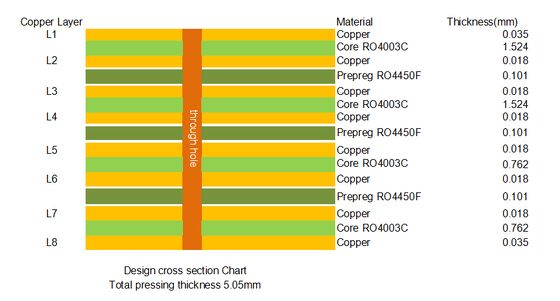
Stack-up PCB
| N. Strato |
Descrizione |
Spessore |
| 1 |
Strato di rame — L1 (Esterno superiore, rame finito 1OZ) |
0,035 mm |
| 2 |
Core RO4003C |
1,524 mm |
| 3 |
Strato di rame — L2 (Strato interno, rame finito 0,5OZ) |
0,018 mm |
| 4 |
Prepreg RO4450F |
0,101 mm |
| 5 |
Strato di rame — L3 (Strato interno, rame finito 0,5OZ) |
0,018 mm |
| 6 |
Core RO4003C |
1,524 mm |
| 7 |
Strato di rame — L4 (Strato interno, rame finito 0,5OZ) |
0,018 mm |
| 8 |
Prepreg RO4450F |
0,101 mm |
| 9 |
Strato di rame — L5 (Strato interno, rame finito 0,5OZ) |
0,018 mm |
| 10 |
Core RO4003C |
0,762 mm |
| 11 |
Strato di rame — L6 (Strato interno, rame finito 0,5OZ) |
0,018 mm |
| 12 |
Prepreg RO4450F |
0,101 mm |
| 13 |
Strato di rame — L7 (Strato interno, rame finito 0,5OZ) |
0,018 mm |
| 14 |
Core RO4003C |
0,762 mm |
| 15 |
Strato di rame — L8 (Esterno inferiore, rame finito 1OZ) |
0,035 mm |
| Spessore totale pressato |
5,05 mm |

Linee guida per la lavorazione di schede multistrato RO4003C
Stoccaggio
I laminati RO4003C completamente rivestiti devono essere conservati a temperatura ambiente (compresa tra 10-32°C). Si consiglia di implementare un sistema di gestione dell'inventario "first-in-first-out" e di stabilire un metodo per tracciare i numeri di lotto dei materiali durante tutto il processo di produzione PWB e la consegna dei circuiti finiti. Questa pratica aiuta a mantenere la stabilità delle prestazioni del materiale RO4003C e garantisce la tracciabilità della qualità di lavorazione.
Preparazione strato interno
Attrezzatura
I laminati RO4003C sono compatibili con una varietà di sistemi di attrezzaggio con perni e senza perni. La scelta tra perni rotondi o scanalati, perni esterni o interni, attrezzaggio standard o multiline, e punzonatura pre-etch o post-etch dipende dalle capacità e preferenze della struttura di produzione del circuito, nonché dai requisiti di allineamento finali. Nella maggior parte dei casi, perni scanalati, un formato di attrezzaggio multiline e punzonatura post-etch sono sufficienti per soddisfare i requisiti, garantendo efficacemente l'accuratezza dell'allineamento degli strati interni delle schede multistrato RO4003C e minimizzando gli errori di lavorazione.
Preparazione superficiale per la lavorazione del fotoresist e l'incisione del rame
La preparazione superficiale del rame per l'imaging fotografico può essere ottenuta tramite processi chimici o meccanici, a seconda dello spessore del core RO4003C. I core RO4003C più sottili dovrebbero essere preparati utilizzando un processo chimico che include pulizia, micro-incisione, risciacquo con acqua e asciugatura per prevenire danni meccanici al materiale del core. I core RO4003C più spessi possono essere lavorati con sistemi di spazzolatura meccanica, che rimuovono efficacemente i contaminanti superficiali e migliorano l'adesione del fotoresist.
I materiali RO4003C sono compatibili con la maggior parte dei fotoresist liquidi e a film secco. Una volta modellati, possono essere lavorati utilizzando sistemi di sviluppo, incisione e rimozione (DES) comunemente utilizzati per materiali FR-4, riducendo i costi di modifica delle attrezzature e migliorando l'efficienza di lavorazione delle schede multistrato RO4003C.
Trattamento ossido
I core RO4003C possono essere sottoposti a qualsiasi processo di trattamento con ossido di rame o alternativa all'ossido in preparazione per l'incollaggio multistrato. Il metodo di trattamento ottimale è tipicamente quello raccomandato nelle linee guida fornite con il sistema di prepreg o adesivo selezionato. Un corretto trattamento ossido migliora la resistenza di incollaggio interstrato delle schede multistrato RO4003C e ne garantisce l'affidabilità.
Incollaggio multistrato
I laminati RO4003C sono compatibili con numerosi sistemi adesivi termoindurenti e termoplastici. Si raccomanda di fare riferimento alle linee guida del sistema adesivo per i parametri del ciclo di incollaggio (come temperatura, pressione e durata) per garantire che la qualità di incollaggio delle schede multistrato RO4003C soddisfi i requisiti e per evitare difetti come la delaminazione.
Considerazioni sulla foratura
Materiali di ingresso standard (alluminio o fenolico pressato sottile) e materiali di uscita (fenolico pressato o pannello in fibra) possono essere utilizzati durante la foratura di core RO4003C o assemblaggi RO4003C in stack a strato singolo o multistrato. La selezione di materiali di ingresso e uscita appropriati riduce l'usura delle punte da trapano, migliora la qualità delle pareti dei fori delle schede RO4003C e previene sbavature e altri difetti agli ingressi e alle uscite dei fori.

 Il tuo messaggio deve contenere da 20 a 3000 caratteri!
 Italian